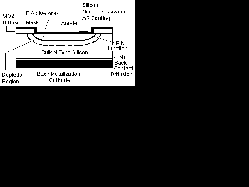
A cross section of a typical silicon photodiode is shown in the figure. N type silicon is the starting material. A thin "p" layer is formed on the front surface of the device by thermal diffusion or ion implantation of the appropriate doping material (usually boron). The interface between the "p" layer and the "n" silicon is known as a pn junction. Small metal contacts are applied to the front surface of the device and the entire back is coated with a contact metal. The back contact is the cathode, the front contact is the anode. The active area is coated with either silicon nitride, silicon monoxide or silicon dioxide for protection and to serve as an anti-reflection coating. The thickness of this coating is optimized for particular irradiation wavelengths. As an example, a Centro Vision Series 5-T photodiode has a coating which enhances its response to the blue part of the spectrum.
The characteristics of pn junctions are well known. However, photodiode junctions are unusual because the top "p" layer is very thin. The thickness of this layer is determined by the wavelength of radiation to be detected. Near the pn junction the silicon becomes depleted of electrical charges. This is known as the "depletion region". The depth of the depletion region can be varied by applying a reverse bias voltage across the junction. When the depletion region reaches the back of the diode the photodiode is said to be "fully depleted". The depletion region is important to photodiode performance since most of the sensitivity to radiation originates there.
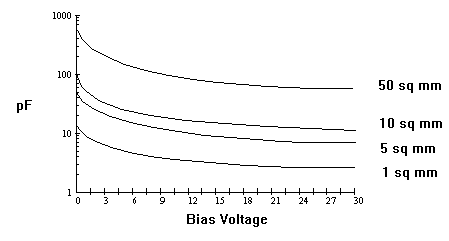
The capacitance of the pn junction depends on the thickness of this variable depletion region. Increasing the bias voltage increases the depth of this region and lowers capacitance until the fully depleted condition is achieved. Junction capacitance is also a function of the resistivity of silicon used and active area size. The relationship between junction capacitance, bias voltage and area is shown in the graph below.
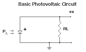
When light is absorbed in the active area an electron-hole pair is formed. The electrons and holes are separated electrons passing to the "n" region and holes to the "p" region. This results in a current generated by light (usually abbreviated Isc). The migration of electrons and holes to their respective region is called "The Photovoltaic Effect".
Silicon photodiodes are most useful as current generators although a voltage is also generated by illumination. Most of the data supplied in this manual refers to the short circuit current characteristics of the photodiodes. The short circuit current is a linear function of the irradiance over a very wide range of at least seven orders of magnitude. The Isc is only slightly affected by temperature, varying less than 0.2% per degree C for visible wavelengths. A recently published independent laboratory study has shown Centro Vision photodiodes to have Isc stability better than +/-0.25% per year.
| Part Number | Sunlight at Noon, mA | Room Light On Table, microA | Super Red LED at 10 mA, 1 CM Away , microA | Laser Pointer @ 1 meter, mA |
| OSD1-5T | 0.47 | 0.45 | 0.32 | 0.71 |
| OSD5-5T | 1.80 | 2.10 | 1.70 | 1.00 |
| OSD15-5T | 4.50 | 5.60 | 2.60 | 1.00 |
| OSD35-5T | 11.00 | 14.00 | 3.80 | 1.10 |
| OSD60-5T | 28.00 | 39.00 | 7.20 | 1.10 |
It must be noted that when a reverse bias is applied some current will flow without illumination. The "dark current" is specified for every device. In cases where a very low bias voltage is used, shunt resistance is specified. This is determined by measuring dark current with +/-0.010 volts applied bias.
In the photovoltaic and zero bias modes, the generated current or voltage is in the diode forward direction. Hence the generated polarity is opposite to that required for the biased mode.
Operating under ideal conditions of reflectance, crystal structure and
internal resistance, a high quality silicon photodiode of optimum design
would be capable of approaching a Q.E. of 80%. The following reference
table identifies, at a Q.E. of 100%, the responsivity of an ideal photodiode
over the 200-1100 nm wavelength range. It should be noted that a Q.E. of
100% is not attainable.
| Wavelength, nm | Responsivity at 100% Q.E. A/W |
| 200 | 0.161 |
| 300 | 0.242 |
| 400 | 0.323 |
| 500 | 0.403 |
| 600 | 0.484 |
| 700 | 0.565 |
| 800 | 0.645 |
| 900 | 0.726 |
| 1000 | 0.806 |
| 1100 | 0.887 |
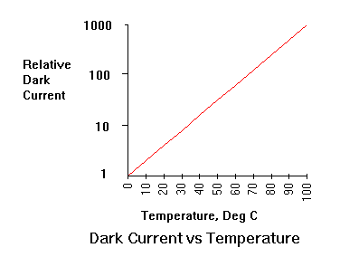
The second change is caused by exponsntial increases in the thermally excited electron-hole pairs resulting in increasing dark current. This leakage doubles for each 8 to 10 deg C temperature increase, as shown below:
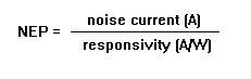
The NEP is dependent on the bandwidth of the measuring system; to remove this dependence the figure is divided by the square root of the bandwidth. This gives the NEP the units of watts/HzE-0.5. Since the photodiode light power to current conversion depends on the radiation wavelength, the NEP power is quoted at a particular wavelength. The NEP is non-linear over the wavelength range, as is responsivity.
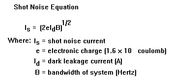
The noise generated by a silicon photodiode, operating under reverse bias, is a combination of shot noise, due to dark leakage current, and Johnson noise due to the shunt resistance of the device and the ambient temperature. The Shot Noise current produced by the reverse leakage current of a device is given by the formula:
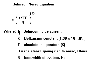
The Johnson noise contribution is provided by the shunt resistance of the device, series resistance and the load resistance. The Johnson noise is given by:
The total noise current is the root mean square sum of the individual noise current contributions.
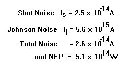
As an example: If a photodiode has a dark leakage current of 2 nA and a shunt resistance of 5E8 Ohms, and a responsivity of 0.5 A/W, and letting the bandwidth of the system be 1 Hz,
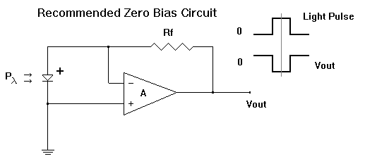
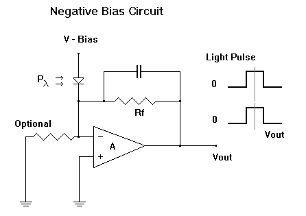
Shot noise is the dominant component of the noise current of a reverse-biased photodiode. This is particularly true at higher voltages. If devices are operated in a photovoltaic mode with zero bias, the Johnson noise dominates, as dark current approaches zero. When operating in the zero bias mode the noise current is reduced such that the NEP, and hence the minimum detectable signal, is reduced in spite of some loss of absolute sensitivity.
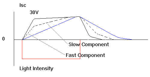
When a photodiode is operated in the unbiased mode, the slow diffusion component dominates, giving risetimes on the order of 0.5 microseconds.
For a fast response time, silicon resistivity and operating voltage must be chosen to produce a depletion layer within which the majority of the carriers are generated. In this case the transit time will be dependent on both the electron and hole drift velocities. The depletion depth necessary for full absorbtion increases rapidly with operationg wavelength. Response times increase correspondingly. This makes it difficult to achieve risetimes faster than 15-20 ns at 1064 nm, whereas risetimes of less than 2 ns are obtainable below 900 nm.
The Centro Vision -3T and -4X series take advantage of the increase in drift velocity resulting from a very high electric field. In this structure silicon thickness is reduced to just contain the required depletion depth, and a heavily doped back layer is used to supply the necessary charge to support the depletion region at higher voltage. In this way the operating field, and hence the carrier drift drift velocities, may be increased without a significant increase in depletion depth. Further increase in speed may be obtained at the expense of overall sensitivity by using silicon which is not thick enough to allow full absorbtion of incident radiation.
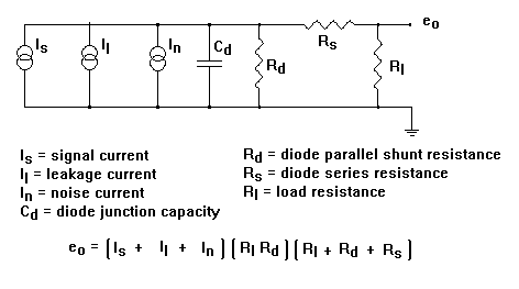
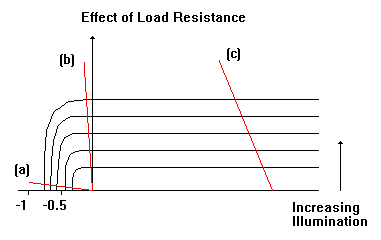
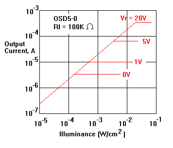
Fundamentally a photodiode is a current generator. The junction capacitance of the photodiode depends on the depletion layer depth and hence bias voltage. The value of the shunt resistance is usually high (megohms). The series resistance is low. The effect of the load resistor value on the current/voltage characteristics is shown in the following figure: